© Paul E. Bennett. 1994, 1998
® All rights reserved Paul E. Bennett 1994, 1998
No liability whatsoever is accepted by Paul E. Bennett
for any errors or ommission in the presented material as published in
Forthwrite, the newsletter of the Forth Interest Group (UK) or on the
Forth Interest Group Websites.
by Paul E. Bennett
In the last article I explained the environment that control equipment has to contend with and gave a few examples of the sort of levels of disturbance that an electronic systems engineer will have to be mindful of when designing such equipment. I also covered a couple of instances on reading a digital inputs In this issue I shall describe keypad and keyboard scanning, analogue input circuits and reading analogue inputs.
Keyboards and Keypads are another form of digital input. As the connection to keypads do not generally extend beyond the immediate system case, the input circuitry can be vastly simpler than that presented in the last issue. We still need to use a few protective components but not to any large degree.
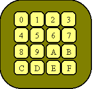
Figure 1: Keypad Matrix
In Figure 1 the keypad is organised as a 4 by 4 matrix. This organisation uses less I/O pins than just reading the 16 switches in parallel but costs in terms of needing a scanning routine. The four switches (labeled C1 to C4) are commutators and may be implemented with transistors, logic level drivers or even relays . The commutator switches are switched on then off in turn to enable the switches in each column to be read into the processor (D0 to D3). The diodes Xn in each keyswitch (0 to F) circuit (inset) prevent any switches in adjacent columns (which may be pressed simultaneously) from passing current when their own column is not activated. The AND gate provides and interrupt signal to the processor (where interrupt driven key press entry is required).
Although this circuit uses eight I/O pins to address 16 switches and does not seem to be much of a saving, some embedded applications are sufficiently restricted for resources where such a saving in I/O pins is worth having. The savings can get much better for larger keyboard arrays.
|
Figure 2: Keypad Layout |
Reading the Matrix The reading technique is generally to enable one column at a time (keeping all other disabled) and then reading the data input port. The collected data is a concatenation of the column commutation drive signals and collected row data and is of the format:-
|
|
Key |
Data |
|
Key |
Data |
|
0 |
11 |
|
8 |
41 |
|
1 |
12 |
|
9 |
42 |
|
2 |
14 |
|
A |
44 |
|
3 |
18 |
|
B |
48 |
|
4 |
21 |
|
C |
81 |
|
5 |
22 |
|
D |
82 |
|
6 |
24 |
|
E |
84 |
|
7 |
28 |
|
F |
88 |
Table 1: Scan Codes
Table 1 shows the scan codes that will be returned from the keypad. To be useful these scan codes will need to be converted to binary coded data, preferably in the order of key value. The conversion implements a priority conversion process, where a one bit on value is converted to a 2 bit binary code. The conversion process can be provided in hardware or software. This entails splitting the nibbles that are the column drives and the returned row data. On the assumption that the above input is being used in a microcontroller whose digital I/O can be selectively placed in input or output mode by setting bits in a control register the following code would scan the keypad.
Code Snippets
HEX 8000 CONSTANT CONTROL-REG : INIT-KPAD (S -- ) : KP-INT-ENABLE (S -- ) : KP-COL-READ (S col-mask -- row-bits) : BITS? (S #\mask -- flag ) : << (S n\places -- n<< ) \ Left Shift n by places : KP@ (S -- kp-bits ) \ Collect all keypad bits in a cell VARIABLE KPS : NEWKEY? (S -- new-key-bits) \ Get the new key value : KEYVAL (S key-bits -- key-code ) \ Return pressed key code. : (KEYPAD) (S -- key-code) \ Wait for and return a key value |
The words INIT-KPAD, KP-INT-ENABLE and (KEYPAD) are the main interface words the programmer will use. INIT-KPAD should be included in the system initialisation. The word KP-INT-ENABLE is only to be used when operating the keypad in interrupt driven mode. This will entail setting the interrupt facility up and using (KEYPAD) in the interrupt service routine. KP-INT-ENABLE will need to be used after each use of (KEYPAD) to set up again for the interrupt so the ISR will look something like:-
: KP-ISR (KEYPAD) KP-INT-ENABLE ;
By non-interrupt driven methods (KEYPAD) could be used as the run-time word in the Forth word KEY. Assuming KEY was a deferred word:-
ASSIGN (KEYPAD) TO-DO KEY
Analogue inputs change the voltages and currents from continuously variable sensors into a digital value suitable for the computers processor. This change occurs in an Analogue to Digital Converter (ADC). ADCs come in various forms and the most common accept a variable DC voltage as input.
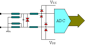
Figure 3: Analogue Input
A Quick Tour Round the Input
The circuit of Figure 3 shows a differential input ADC which, like the digital input shown last issue, has been given a measure of protection from external transients. For the analogue circuit, component values and types have to be selected very carefully, especially if the signals are meant to monitor a signal with a high frequency content. In the process control industry though, the analogue signals are in the main voltage or current derived. The circuit of Figure 3 is measures the value of a DC voltage input. To measure the level of an AC signal suitable AC to DC conversion (bridge rectifier and smoothing) will need to be added.
The analogue voltage based signals used within industry are usually in the range from 10 to 50V. These may be positive or negative with respect to ground and dealing with negative values is wholly dependent on the set-up of the ADC. The first bank of resistors in conjunction with the Transorb are front line protection from excessive voltage levels. The second bank of resistors further reduce the voltage to levels that the ADC itself is capable of accepting.
Why a Differential Input?
The reason I am showing you just a differential input is that these are generally more useful in an industrial setting. A differential input, fed a voltage from a sensor over a twisted pair cable will have less differential noise than a single pole input that must rely on the grounding connection (which will probably be very noisy already). To be fair, most ADC’s on micro-controllers have unipolar inputs, but it is good practice to precede these with a small operational amplifier circuit to protect the microprocessor. Such operational amplifiers will have differential inputs.
Can the input be isolated?
Isolating analogue inputs is trickier than isolating digital inputs especially if there is a varying DC component. There are devices around which enable isolated analogue inputs to be constructed (Opto-isolators with light-based feedback) and techniques which rely on changing a DC voltage to a variable frequency signal (which can then be transformer isolated). Alternatively, a number of digital Opto-isolators could be interposed between the ADC and the data bus of the microprocessor. Analogue Isolation becomes an issue that must be viewed on a system cost/accuracy/benefit basis.
Another kind of analogue
Not all analogue signals are AC or DC levels. There are also frequency or phase domain signals which are derived from Quadrature detectors, Resolvers or Synchro’s, and oscillatory circuits whose frequency of operation is modulated by a change of capacitance or inductance as the physical measurand changes. The level of the signals often remain constant and only the relationship of phase or frequency varies. These are easier to isolate as the signals will pass through transformers easily and, in some cases, can also be digitised by clipping and passed through Opto-isolator inputs. For many of the analogue input types there are a variety of specialised circuits which take most of the hard work out of developing an interface. I am not going to cover them in this series as there are far too many of them to be done justice owing to the wide variety of ways analogue values can be collected.
Digital Representation of Analogue Values
Having got the conversion from analogue to digital representation organised there comes the question of value representation and manipulation. The value will need proper scaling and preparation for display. If you have a 10 bit ADC should the values it presents be arranged towards the MSB or towards the LSB. This will rather depend on what you may wish to do with the data once it is collected. Some microcontrollers, like the MC68HC16, give the programmer the choice.
LSB biased representation
Sticking with a 10 bit ADC input (D0 to D9 and a sign bit) the LSB biased representation would be organised so that the LSB of the ADC (D0) corresponds to data bit 0 and the MSB (D9) is corresponds to data bit 9. The Sign bit would normally be wired to data bit 15.
|
15 |
14 |
13 |
12 |
11 |
10 |
9 |
8 |
7 |
6 |
5 |
4 |
3 |
2 |
1 |
0 |
|
S |
X |
X |
X |
X |
X |
D9 |
D8 |
D7 |
D6 |
D5 |
D4 |
D3 |
D2 |
D1 |
D0 |
This means that the numerical value of the analogue input requires no real modification, the math’s for averaging is kept simple though scaling will require a multiplication and division with the Forth word */ which may take some time on a small microcontroller.
MSB biased representation
With the MSB biased representation we are dealing with natural binary numbers. This category of numbers are interesting in that they can be scaled very simply by a single multiplication operator.
|
15 |
14 |
13 |
12 |
11 |
10 |
9 |
8 |
7 |
6 |
5 |
4 |
3 |
2 |
1 |
0 |
|
D9 |
D8 |
D7 |
D6 |
D5 |
D4 |
D3 |
D2 |
D1 |
D0 |
0 |
0 |
0 |
0 |
0 |
0 |
The Forth word UM* is best for this on a single cell value as you can just grab the full scale value and multiply it with UM* then NIP to retain the upper 16 bits of the resultant double cell value. In the example below we shall assume that with an MSB biased ADC input the range of value to be displayed should be from 0 to +100
HEX : .VALUE (S -- ) |
I will leave it as an exercise for the reader to resolve a display with a scaling from -100 to +100.
This concludes the input side and the Reading the World series but next issue we begin the Writing the World series which will deal with control outputs.