© Paul E. Bennett. 1994, 1998
® All rights reserved Paul E. Bennett 1994, 1998
No liability whatsoever is accepted by Paul E. Bennett
for any errors or omission in the presented material as published in
Forthwrite, the newsletter of the Forth Interest Group (UK) or on the
Forth Interest Group Websites.
by Paul E. Bennett
It is often the case that some form of timed pulse output is required. This may be for driving larger devices such as motors using PWM (pulse width modulated) techniques. We usually want to read inputs constantly to determine if the output we are performing remains valid. Output without feedback is not control. Therefore this article is going to concentrate on the timing aspects and present a PWM output stage which can be used for driving DC motors.
As stated above we need to operate carefully with timers. Many software books (especially those for beginners) give timing delay loops in this fashion:-
100 CONSTANT CALIBRATE \ : DELAY (S delay-time --- ) NEXT ; |
used as:-
100 DELAY
However, the problem with the above timing loop is that it does not exit until it is completed. Whilst a PAUSE could be included for multi-tasking environments this can lead to indeterminate timings. If we are to maintain proper control we need a timing strategy that does not hog CPU time and remains reasonably deterministic. We therefore need timers that will exit with a flag which can be checked and a programming style that enables the activity to be incorporated in process loops.
The above code only shows one timer function which relates to the current time clock for the system. However with this method several timer functions could be implemented from just one timer tracking the overall system timings.
There are many ways of generating analogue outputs. The analogue parameter can be voltage, current, frequency, pulse amplitude or pulse width. It would be beyond the scope of this series to give an individual treatment for each one due to the variety of methods that can be employed (doing things digitally is the simple bit but sometimes restricting). Instead I am going to cover just a couple of basic analogue outputs from which others can be developed. I shall start with one type that is becoming very common on microcontroller chips; the PWM output.
PWM Outputs
It may seem strange to classify the PWM output as analogue when it is so easily generated digitally and the output still switches between two distinct voltage levels. However, the analogue value is contained in the pulse duration. Coupled with a simple charge-pump circuit, and suitable filtering, you can convert the pulse duration to an analogue voltage.
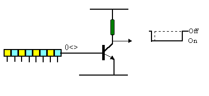
Pulse Width Modulated (PWM) outputs operate on a fixed period basis with just the width of the ON pulse varying. Such outputs used to be generated by analogue means with a sawtooth wave generator and a voltage comparator. However, doing it digitally is much more stable in terms of timing repetition. For this a down-counter and a zero-point detector is required. Whether this function is performed in hardware or software the technique is the same. Preset the down-counter to a value corresponding to the percentage of on-time required for the pulse and turn the output off when zero is reached. If the preset is zero then no pulse is produced.
Figure 1 - Pulse Width Modulated Output
To perform this function purely in software requires that the processor you are using has enough raw speed to manage the necessary frequency of counter clock required to obtain the desired output rate.
DAC (ladder method)
Using digital to analogue converters (DAC) in which a reference voltage is switched through a bank of resistors wired in an R-2R network.
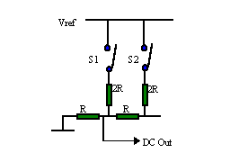
Figure 2 - R-2R Ladder DAC
As each switch is closed (in binary coded patterns) more current flows from the reference voltage to the load resistor. S1 is the most significant bit, in the above diagram, and S2 the least significant. The steps in voltage for the output are in proportion to the binary code applied to the switch closures. In real DAC chips the switches are transistors driven by the logic latches. Using opto-isolators in such a circuit would give an isolated DAC output provided the reference voltage was isolated from the logic supply. The schematic symbol for a DAC is shown below.
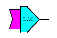
Figure 3 - DAC Schematic Symbol
Finally, for this article, a word of caution about controlling outputs. If you are planning to run machinery off of the controlled outputs (motors, actuators, solenoids etc) be sure to assess the risks associated with the action being performed. A system designer should always be aware of the risks of inadvertent activation of outputs.
In this series we have covered analogue and digital inputs and outputs and issues relating to real world interfacing. This has been just a brief overview and the subject may be explored deeper and wider than those issues presented here, not least in respect of factors such as interference and transient protection. Outputs, like inputs, will also require protection from environmental aspects as discussed in the first article in the series.
With appropriate care, forward planning and awareness of the hazards of dealing with the real world, it is possible to design systems which are certifiably dependable in their expected operational and storage environments.